With the gradual maturity of consumer electronic products in terms of stability and user experience, market competition is gradually shifting from functional innovation to homogenization. In this context, antennas, as a key component of TWS devices, are facing more extreme performance requirements – lightweight, compact, and low-cost antenna solutions are increasingly becoming a necessity.
Among numerous technological routes, LDS antennas have gradually gained recognition from various links in the R&D to supply chain due to their comprehensive performance advantages. Whether it is the pursuit of flexibility and space utilization on the design side, or the control of stability and cost on the quality and procurement side, LDS technology has demonstrated strong adaptability.
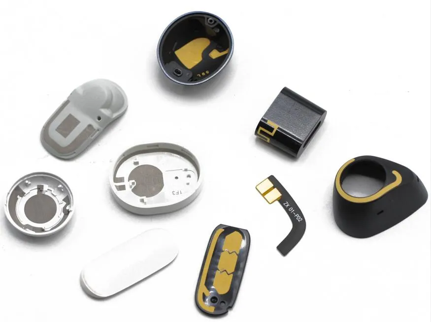
LDS, Laser direct molding technology is an advanced process for directly manufacturing circuit patterns on the surface of injection molded parts. This technology uses laser scanning on the surface of specially modified plastics to activate the organic metal composites, forming a strong metal circuit in the subsequent chemical plating process. This method enables the direct construction of antennas on three-dimensional structural surfaces, greatly enhancing design freedom.
Compared with traditional FPC antennas, LDS can be seen as a “three-dimensional upgrade”. Although FPC has certain flexibility, it still relies on flat stamping forming, making it difficult to achieve efficient layout in highly compact and structurally complex internal spaces. LDS forms precise circuits through laser engraving, which not only fully utilizes irregular spaces such as equipment casings, but also effectively reduces interference with surrounding components, thereby ensuring the stability and consistency of signal transmission.
Top-Link focuses on the research and manufacturing of LDS antennas, accumulating multiple process advantages in technical practice. The antenna products we provide are compact in size and in line with the trend of miniaturization in consumer electronics; The process is highly simplified, covering key steps such as plastic injection, laser activation, and chemical plating, with the characteristics of short cycle and high stability. In terms of accuracy, the circuit line width and spacing can be controlled at the level of 50 µ m, and the laser perforation depth can also reach 0.8-1mm. Combined with advanced RF testing system, it comprehensively guarantees product performance and reliability, providing support for the integration and signal optimization of consumer electronic products