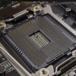
Against the backdrop of rapid advances in AI chips, 5G communications and high-performance computing in 2026, test probes — critical precision components in semiconductor testing — have garnered growing attention across the industry. From smartphones to AI accelerators, every chip undergoes rigorous inspection by test probes before mass production. With the growing adoption of advanced technologies such as Chiplet and 3D packaging, the test probe industry is embracing dual opportunities of technological upgrading and surging market demand. As a professional manufacturer in precision connection and testing in China, Shenzhen Top-link Technology Co., Ltd. boasts years of technical expertise, with independent R&D and mass manufacturing capabilities for test probes, making it a trusted partner in this niche sector.
Test probes are key consumables determining semiconductor yield and testing efficiency. According to Yole and CICC Research, the global wafer test probe market is set for steady growth in the coming years. Rising demand for AI servers and high-performance computing has raised higher requirements for probe precision, reliability and durability. As chip processes advance and packaging complexity grows, probe design is evolving toward finer pitch, higher frequency and greater durability, favoring manufacturers with micro-nano manufacturing capabilities — a segment where Top-link is strategically positioned.
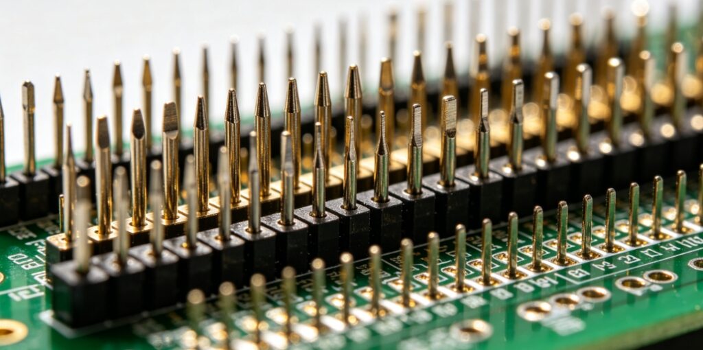
The development trajectory of the test probe industry over the next 3–5 years is taking shape.Demand for high-frequency and high-speed probes is surging. The evolution of 5G and upcoming 6G communications, coupled with the adoption of high-speed interface standards such as PCIe 6.0, demands probes with superior high-frequency signal processing capabilities, posing stricter requirements for material selection and structural design. Furthermore, the trend of device miniaturization drives the development of ultra-fine pitch probes. Applications including microphones, wearables and medical electronics are fueling demand for micro-probes at 0.1mm diameter, a key frontier for probe innovation.
In this promising yet challenging industry, Top-link has forged distinctive technical advantages in test probes through sustained R&D investment and manufacturing capacity building. Responding to industry miniaturization trends, the company achieves mass production of high-precision probes, delivering reliable solutions for semiconductor wafer testing and micro-electronic product inspection. Building on profound expertise in Pogo Pin connectors and high-frequency probes, Top-link optimizes precision structures and materials for AI servers and 5G communication modules, ensuring stable contact resistance and signal integrity.
As the semiconductor industry chain evolves in 2026, the test probe sector is moving from the background to the spotlight. For customers with precision testing needs, Top-link is more than a probe R&D and manufacturing supplier — it is a technical partner providing stable products and professional services in micro-connection and precision testing. Committed to solid technology and reliable quality, Top-link will continue to contribute to the advancement of precision testing technology.